Random signals cannot be predicted. In our example there are 4 states which are identical to the states of a 2-bit.
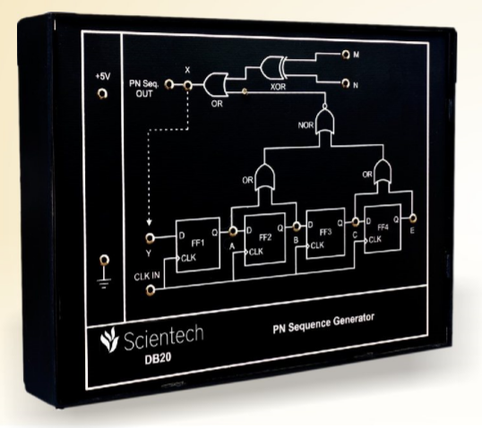
Pn Sequence Generator Amplelab
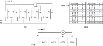
PN sequence is generated at the output of the fourth D type flip-flop.

. The circuit can exhibit chaos in appropriate parameters of capacitance and inductance. Sequence Generator Digital Circuits FSM K-map simplification. The PN Sequence Generator block generates a sequence of pseudorandom binary numbers using a linear-feedback shift register LFSR.
Circuit Design Suite. First count the number of zeros and ones in the given sequence. M is the number of shift.
Where h can be either 1 short circuit or 0 open circuit and xs are the. 101 sequence detector using Verilog. Autocorrelation properties of a PN sequence are.
LFSR is basically a shift register configuration that propagates the. This paper deals with the vital role of primitive polynomials for designing PN sequence generators. This object generates a sequence of pseudorandom binary numbers using a linear-feedback shift register.
Of flip flops can be calculated as N 2n-1 For instance the given. Generation of Pseudo-Noise PN Sequences December 17 2021 The pseudo-noise or pseudo random sequence is a noise like high frequency signal. Fig35 The block diagram of 16 bit LFSR 4.
In t 0 cycle the new sequence is moved in the feedback path is disconnected and the first bit of the new sequence is driven in the next clock cycle. Circuit diagram of pn sequence generator You can generate PN sequence by using shift registers see the diagram. However this one with d flip flops and xor gate did work somewhat.
This signal is binary in nature. The shift register I need to use is the 74LS194. We analyze the dynamics of the circuit including equilibrium points and its stability bifurcation diagram Lyapunov.
The implementation of the LFSR circuit with VLSI technology makes it useful in low-power communication system design. 15th state is the same as zeroth state since the maximum length of PN sequence is 15. Data Acquisition and Control.
Implementation Of PN Sequence Using Vedic Mathematics The two. Request PDF Design of PN sequence generator based on memristor oscillator This paper proposes a very simple chaotic circuit which contains a charge-controlled memristor a capacitor and an. In this way it is just as if the new.
The PN code sequence is a pseudo noise or pseudo-random sequence of 1s and 0s but not a real random sequence. PnSequence commPNSequence creates a pseudonoise PN sequence generator System object. A very simple chaotic circuit which contains a charge-controlled memristor a capacitor and an inductor for generating pseudo random PN sequences shows that the chaotic sequences obtained from the.
The standard LFSR linear feedback shift register used for pattern. And let this number will be N. 1 65535 PN sequence.
Block diagram of the LFSR when m 4 can. Here is the circuit. The block diagram of 16 bit LFSR is shown in Figure 35.
Step 1 At first we need to determine the number of flip-flops which would be required to achieve our objective. Select the high number of the two. I tried doing a PN Sequence generator using a shift register in Multisim but it didnt work.
Contents Flipflops Shift Registers PN Sequence Generator Counters Loadable Counter Clock Division Clock Division by 3 General Approach for Clock Division Sequential Logic Blocks The output of. In t 0 cycle the new sequence is moved in the feedback path is disconnected and the first bit of the new sequence is driven in the next clock cycle. How can I implement a sequence generator that generates the following sequence 0000 1000 0001 0011 0110 1101 1110 1111 using a universal shift register.
PN Sequence Generation PN Sequence Generation A PN data sequence is an M-sequence that is generated using a linear feedback shift-register circuit as illustrated below. In this way it is just as if the new.

Pn Sequence Generation
14 7 Pseudo Random Sequence Generators Engineering360
Simulated Circuit Diagram Of The Desinged Encoder In Figure 3 Driven By Download Scientific Diagram

Circuit Diagram For The Pn Sequence Generator Download Scientific Diagram

Simulated Circuit Diagram Of The Desinged Encoder In Figure 3 Driven By An Pn Sequence Generator

Block Diagram Of Pn Sequence Generator 3 1 3 Bpsk Modulator The Spread Download Scientific Diagram

Hxh9g8skbzo1ym
Pn Sequence Multisim Live
0 comments
Post a Comment